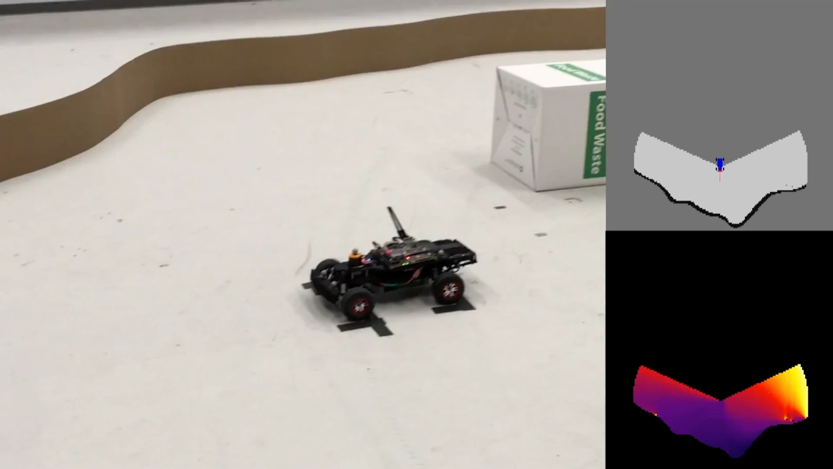
Selecting informative sensor viewpoints
An exploring robot must select viewpoints for subsequent sensor measurements. Shannon mutual information quantifies the expected reduction in map uncertainty from a measurement. Evaluating this quantity across candidate viewpoints guides information-based exploration.
Evaluating many viewpoints requires repeated access to the same map data. The memory organization and processing hardware are co-designed to supply map data for parallel calculations. The prototype uses programmable hardware called a field-programmable gate array (FPGA), whose logic can be configured to test a specialized architecture.
The map is a two-dimensional occupancy grid: each cell stores the probability that a region contains an obstacle. The hardware evaluates the Fast Shannon Mutual Information (FSMI) algorithm for multiple beams from a distance-measuring sensor. It supplies information estimates to a planner, while other robot systems handle motion and map construction.
Memory bandwidth constrains parallel computation
Different sensor beams can be evaluated in parallel, but each processing core needs access to the map. The rate at which memory supplies these values is its memory bandwidth. When bandwidth is insufficient, additional cores spend time waiting for data.
The target FPGA’s standard memory blocks can read two independent addresses per clock cycle. Supplying sixteen cores by replication would require eight complete map copies, substantially increasing storage requirements. The memory architecture instead partitions one map across independently accessible memory banks, providing parallel access without that replication overhead.
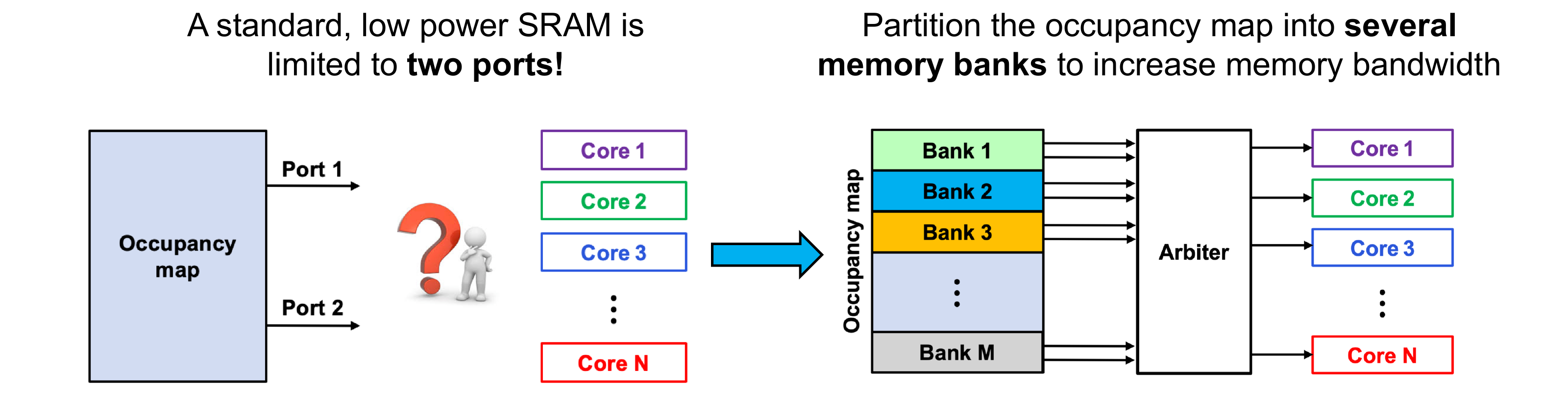
Co-designing map layout and parallel computation
Partitioning the map adds read ports, but the assignment of cells to banks determines how effectively those ports are used. A memory-access conflict occurs when more than two distinct addresses in the same dual-port bank are requested in one cycle. The additional requests must wait.
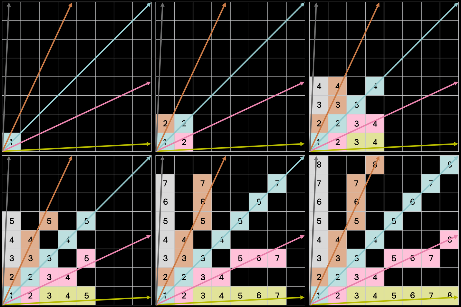
Candidate sensor viewpoints can lie anywhere in the map, so the architecture must accommodate different ray origins and directions. Assigning entire columns or rows to individual banks can concentrate simultaneous requests in one bank. The examples below show this limitation: three rays request different cells from the same bank at cycle 5.
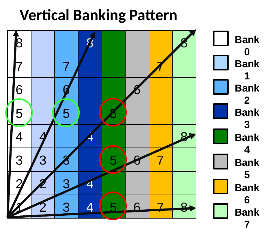
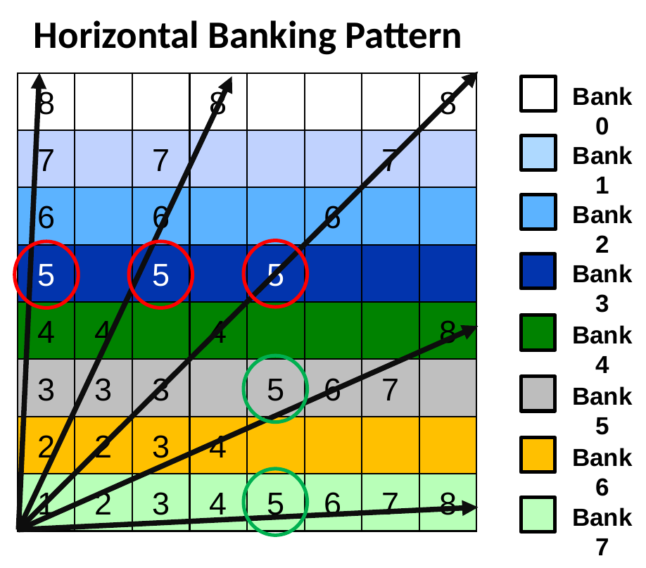
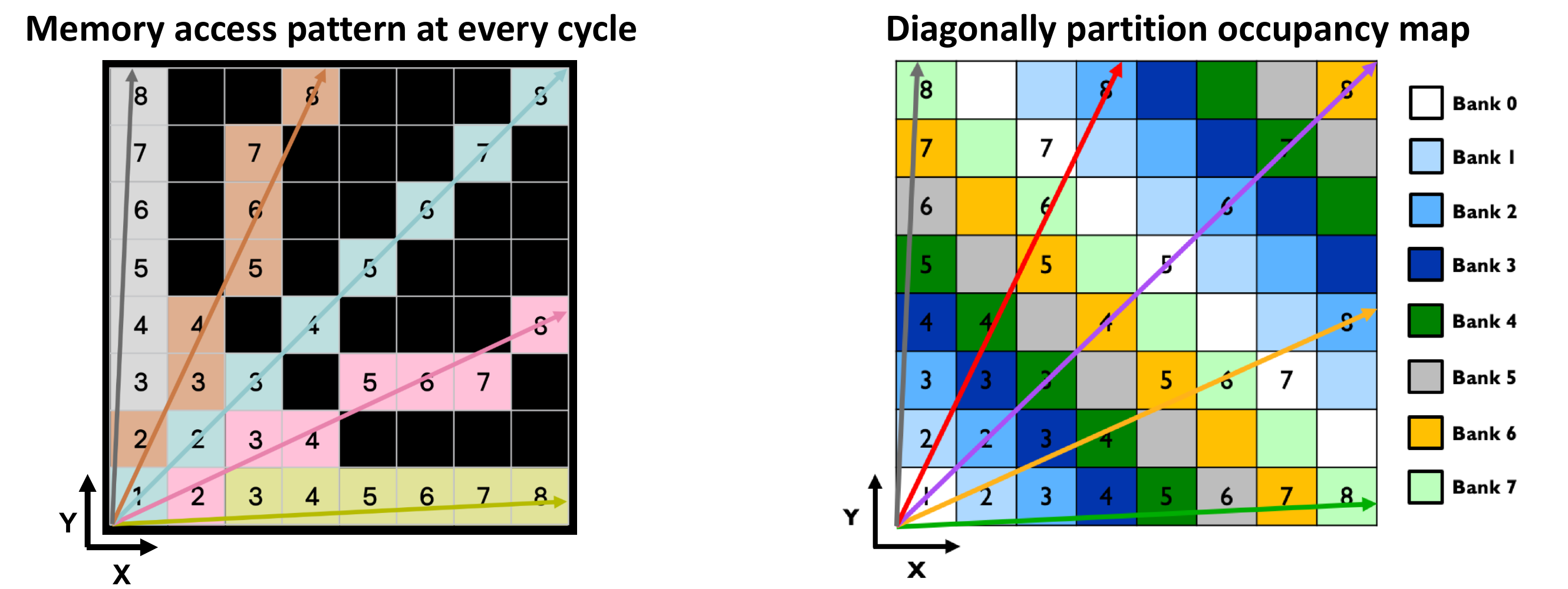
The architecture distributes the map across 16 memory banks in a diagonal pattern chosen for the paths of sensor rays. This arrangement reduces competition for the same bank. An arbiter schedules requests that still conflict. Each address also groups four neighboring cells, supplying more map data per read.
These architectural choices align the map layout with the algorithm’s access pattern and the FPGA’s memory interfaces. The spatial model remains an occupancy grid, while its physical organization supports parallel computation without duplicating the map. The animation and companion diagram show how sensor rays traverse the grid and how the banks distribute their accesses.
Evaluation and limits
The FPGA prototype runs at 62.5 MHz on a Xilinx Zynq-7000 XC7Z045 device. It evaluates a complete 200-by-200-cell information map twice per second (2 Hz). This grid covers 20 m by 20 m at 0.1 m resolution. The 2 Hz rate refers to complete information-map evaluations for viewpoint selection. It does not describe camera capture, robot control, or occupancy-map construction.
The published comparison reports roughly two orders of magnitude faster computation than a single-threaded FSMI implementation on an Intel Xeon E5-4627 v2. That CPU runs at 3.4 GHz. The paper reports approximately 2 W for the FPGA implementation. Its resource table specifies 1.977 W of dynamic power. The CPU comparison uses approximately 22 W above its idle power. These figures describe the evaluated computation, rather than total robot or board power.
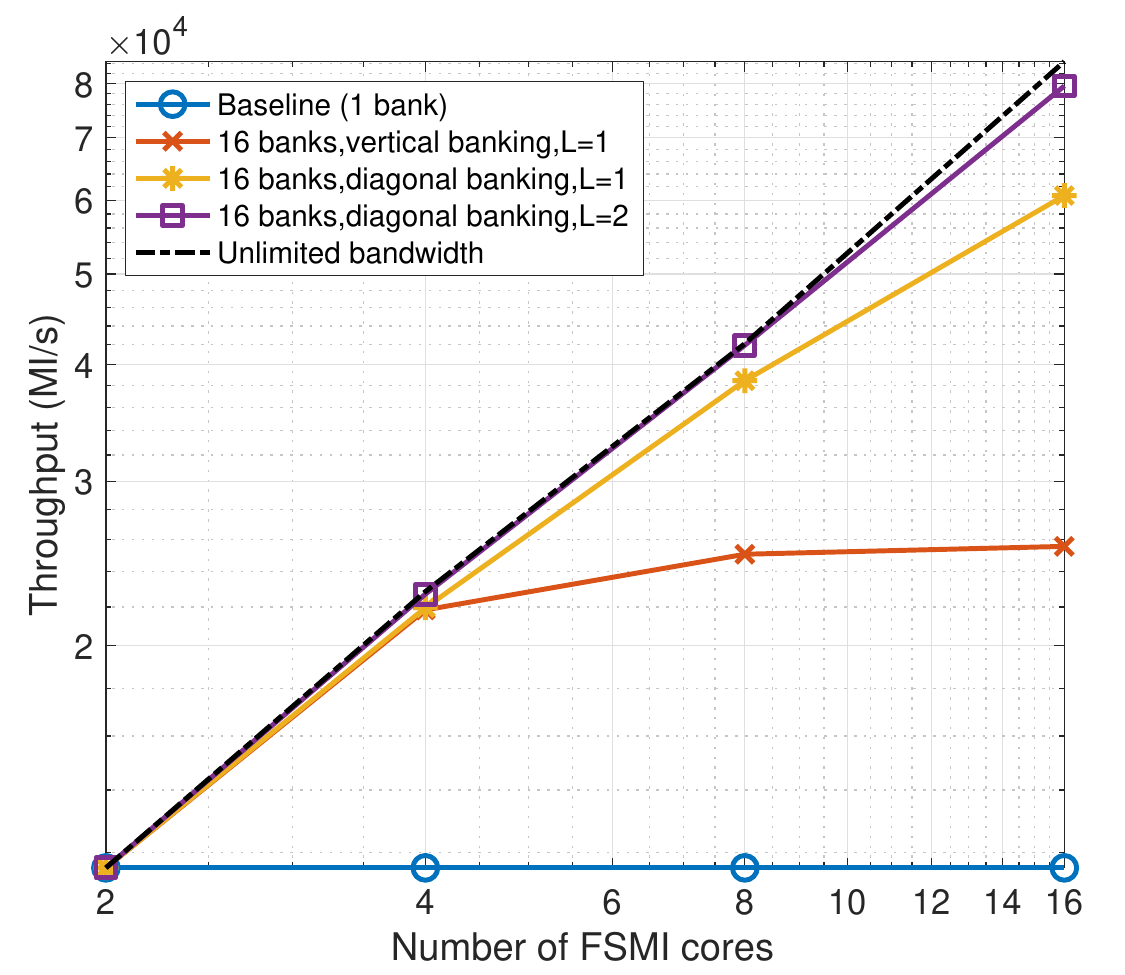
The throughput comparison shows why memory organization matters as core count increases. A single bank limits the benefit of additional cores, while diagonal banking with two-by-two packing approaches the unlimited-bandwidth reference. Under the evaluated scan configurations with 200-cell beams, computation time is less than 6% above that reference. The architecture supports up to 512 by 512 map cells.
Near-optimal banking for the SRC extension
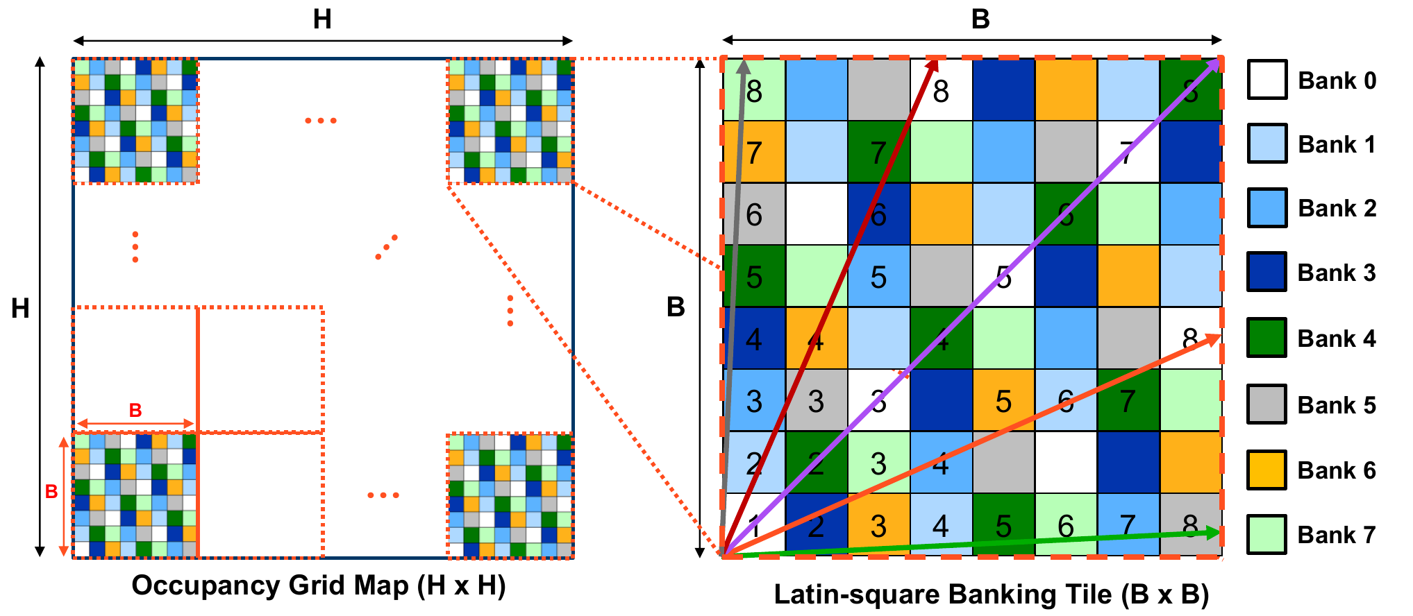
The diagonal layout raises a broader question: how should map cells be distributed to minimize competition for memory? For the ACM Student Research Competition extension, I analyzed Latin-square banking patterns. Within each repeating tile, every row and column uses each bank once, distributing accesses across the available banks.
I proved that this family is near-optimal for memory-access conflicts under the analyzed ray-access model. The result applies as the number of beams from one scan location and one angular region tends to infinity. This analysis connects the geometry of map access to a principled choice of memory layout.
The SRC extension also evaluates how banking and request scheduling work together. In the cycle-accurate ASIC simulation below, Latin-square banking increases throughput by distributing requests more evenly. A priority arbiter further reduces delays by selecting which pending requests each bank serves.
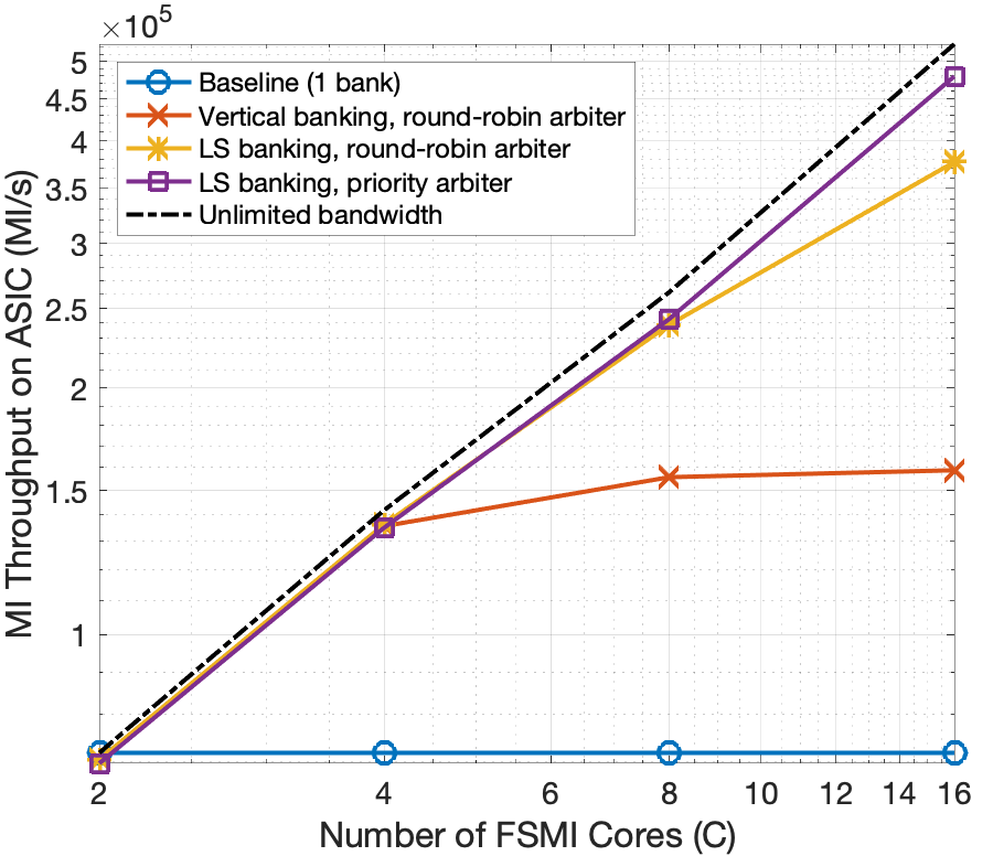
At 16 cores, vertical banking with round-robin scheduling reaches approximately 30% of the reference throughput. Latin-square banking raises this to approximately 72%; adding priority scheduling raises it to approximately 91%. These simulated results illustrate the combined effect of memory layout and scheduling. They complement the near-optimality analysis and are separate from the RSS FPGA evaluation above.
Continuous mutual information
The RSS prototype and the IROS 2021 follow-up are separate hardware designs. Keshav Gupta, Peter Li, Sertac Karaman, and Vivienne Sze developed the IROS accelerator for map-scale continuous mutual information. It evaluates all cells in a 201-by-201 grid in 1.55 ms using 1.7 mJ per evaluation on a Zynq-7000 FPGA. These results belong to the continuous formulation evaluated at IROS 2021.
ACM recognition
For this SRC extension, I received the gold medal at the ACM Student Research Competition at MICRO-52 (2019). I subsequently received first place in the graduate category of the 2020 ACM Student Research Competition Grand Finals. The recognized project was “A Mutual Information Accelerator for Autonomous Robot Exploration.” Official ACM Grand Finals results; official ACM MICRO-52 results; ACM announcement.
The RSS spotlight presentation begins at 2:46:02 in the conference recording.
Cite this work
High-throughput Computation of Shannon Mutual Information on Chip
BibTeX
@inproceedings{li2019rss,
  author = {Li, Peter Zhi Xuan and Zhang, Zhengdong and Karaman, Sertac and Sze, Vivienne},
  title = {High-throughput Computation of Shannon Mutual Information on Chip},
  booktitle = {Robotics: Science and Systems},
  year = {2019}, doi = {10.15607/RSS.2019.XV.058},
  note = {First two authors contributed equally}
}